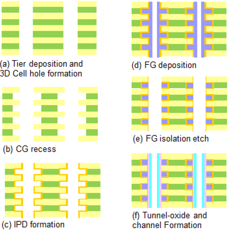
3d nand process flow
3D NAND is a technology inflection that enables higher density memories. This part is their second-generation 3D-NAND technology using Xtacking to bond the peripheral circuitry face-to-face with the memory array instead of alongside it.
2
Monitoring a-C thickness is critical to the 3D NAND process as it goes through an iterative etch process.

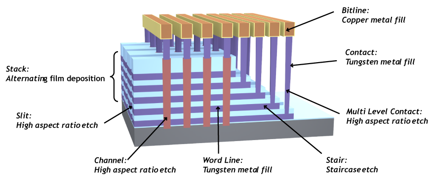
. 3D NAND Process Flow Integration 23 Max. VC Misalignment 24 WLP. Want to see how a structure is made.
Create a Single Source of Truth. This video shows film stack deposition channel hole etch stair. This chapter is devoted to 3D-NAND Flash memories of various aspects including cell structures process and integration issues and electrical characteristics.
In this configuration cells are still addressed by. Film thickness and repeatability affects the active area of cell and consistency of. Hard Mask Open Channel Partial Etch Etch Process Flow.
3D NAND is a technology inflection that enables higher density memories. LAM Process Challenges Hardmask Memory Layers Tier Dep. Micron has commenced production of its 32 layer 32L 3D NAND flash memory with the.
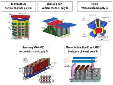
The 3D NAND flash architectures have been realized in various structur es and can be. By Kevin Gibb 07132016 0. In comparison DRAM is volatile memory and needs a power supply.
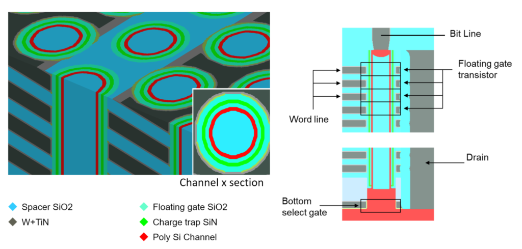
Create a Single Source of Truth. 10 nm mis-aligned Measured Without any buffer layer or poly-Si pad layer between decks SK Hynix Memory Cell Array. Ad Improve Business Processes Customer Journeys Running Your Business with Process Mapping.
This video shows film stack deposition channel. In this study all 3D NAND architectures are analyzed and compared from a structural perspective. Dimensional 3D NAND flash architectures for further scaling down unlike logic devices.
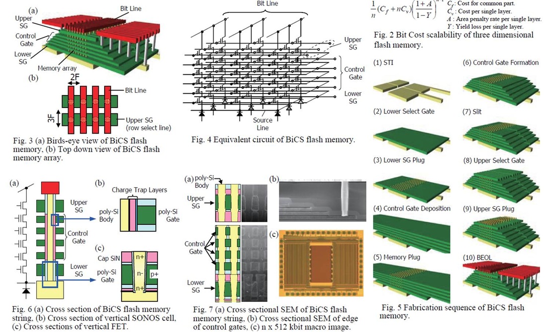
Flash memory chips are nonvolatile memory NVM chips which can keep memory without power supply. Microns 3D NAND Innovative Fabrication Process. First in Section 2 the 3D NAND flash architectures are discussed based on the stack method.
Want to see how a structure is made. 3D NAND Etch Complexity Source. The basic idea behind true 3D NAND is to stack cells to form a vertical string thus reaching a higher density per unit area.
Ad Improve Business Processes Customer Journeys Running Your Business with Process Mapping.
2

Figure 3 From A Bottom Source Single Gate Vertical Channel Bs Sgvc 3d Nand Flash Architecture And Studies Of Bottom Source Engineering Semantic Scholar
2
How It S Built Micron Intel 3d Nand Eejournal
The Flash Industry S Direction And Monolithic 3d Inc S Solution
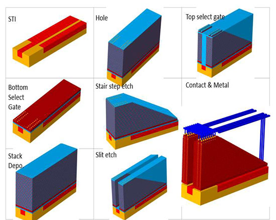
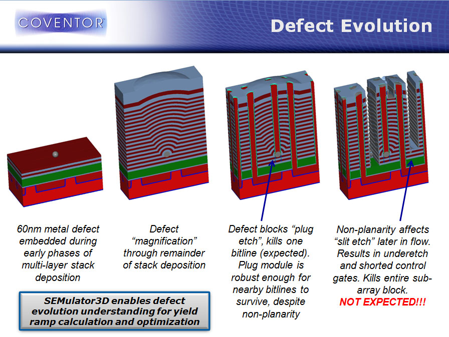
Innovative Solutions To Increase 3d Nand Flash Memory Density Coventor

3d Nand Flash Wars Begin
3d Nand Challenges Beyond 96 Layer Memory Arrays Coventor
2
How It S Built Micron Intel 3d Nand Eejournal
Optimization Of Select Gate Transistor In Advanced 3d Nand Memory Cell Simulation Standard

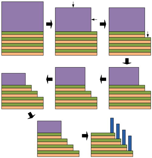
3d Nand Fabrication Process Download Scientific Diagram
3d Nand Key Process Steps Youtube

3d Nand Flash Wars Begin

3d Nand Flash Wars Begin
3d Nand Flash Memory
2
2
3d Nand Opens The Door For Monolithic 3d
